HIOS Highly Integrated Optoelectronic Sensor

An EU funded project. FAST TRACK TO INNOVATION.

background.

From personal mobile devices, to wearables, smart homes, offices, cars, and more, people consistently are exposed to and surrounded by sensors. Sensor functionality is evolving rapidly, from making our phones more intuitive and lighting solutions more intelligent to conserving battery power and enabling breakthrough medical technologies.

read more...
From personal mobile devices, to wearables, smart homes, offices, cars, and more, people consistently are exposed to and surrounded by sensors. Sensor functionality is evolving rapidly, from making our phones more intuitive and lighting solutions more intelligent to conserving battery power and enabling breakthrough medical technologies. Sensors therefore play a key role in many applications in fields such as mobile and consumer, automotive, or industrial. One thing is constant across the fields: the challenging demand for high performance (high sensitivity, low power consumption,…) often in combination with small size and low cost. This drives the need for sensor integration with electronics and other system coponents. For a sensor solutions provider like ams AG and process- and equipment suppliers like APC, Boschman and Bühler this means that they have to be at the forefront of sensor integration to be competitive in their respective markets, a goal that can only be achieved by close collaboration.

idea.

HIOS – “Highly Integrated Optoelectronic Sensor” addresses this need for collaborative innovation for the growing market for intelligent light sensors. In particular HIOS aims to develop and launch the world’s first light sensor with fully integrated optical stack, including multiple filters, lenses and an aperture replacing multiple discrete components.

read more...
HIOS – “Highly Integrated Optoelectronic Sensor” addresses this need for collaborative innovation for the growing market for intelligent light sensors. In particular HIOS aims to develop and launch the world’s first light sensor with fully integrated optical stack, including multiple filters, lenses and an aperture replacing multiple discrete components. The 3D sensor, IC filter and Wafer Level Optics integration technology developed in the HIOS project will be the enabler to bring cost-efficient, very small, and high-performance sensor to the market but can also be applied to multiple other sensor applications. For this reason a high-volume production environment for 3D / Through Silicon Via (TSV) has been set up by ams AG which is now extended by equipment and processes for on-chip inorganic optical filters and wafer level molding to form on-chip optical components

markets.

Initially addressed market opportunity lies in growth markets that have a high demand for low size and/or low cost, but cannot compromise on quality, and are therefore a perfect fit to the HIOS products. The three main markets are:
Wearable Market, Low Cost Consumer Market (smart phones, cellular), Smart Lighting Market.

Expected Output

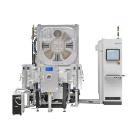
The output of the project will be products with integrated lenses and apertures, and specifically designed filters, as well as equipment and process enhancements. Specifically, the  world’s first light sensor with fully integrated optical stack meeting tighter specifications (footprint, height) than any prior art at substantially lower cost, a filter deposition tool for volume manufacturing achieving industry’s tightest filter specifications, and a Wafer Level Molding manufacturing equipment with new alignment system for tightest known alignment tolerances will be key innovations resulting from HIOS.

Objectives

1.

Wafer Level Molding with best-in-class alignment accuracy and process control

2.

Tailored Filter design with tightest pass band width control; low stress filter deposition to enable multiple filters

3.

Light sensors of smallest size and lowest system cost at best optical performance simplifying assembly and enabling a new class of very thin consumer products

partners.

Consortium as a whole

HIOS is a project proposal with a vertical supply chain involved. The partners complement each other in a well-balanced and structured way and combine capabilities and infrastructure to bring technology to market: ams has high technology competence in wafer processing, optical sensor solutions, and 3D integration and related technology. The 3D heterogeneous integration concept (TSV & RDL) has a central role, as it is needed to enable the wafer level molding process. Together with wafer level bumping, a miniaturization and cost reduction can be reached. The main tasks of Boschman in the HIOS project is the development of the film-assisted Wafer-level molding (FA-WLM) technology and related equipment modules for SIP modules with integrated sensors.

read more...
The equipment is based on existing Boschman molding systems, but as FA-WLM is a novel technology for this application, new equipment will have to be developed. A main innovation will be the integration of an alignment system, reaching the required tight tolerances for the first time, bringing Boschman into a unique market position. APC will be involved in the engineering tasks of the new FA-WLM equipment, including engineering of the mold tools. Further, APC will develop the tailored molding process on the novel system. Bühler will improve the filter application process and develop corresponding new filters, to reliably achieve the targeted tight filter specification with high accuracy and yield. The targets of the HIOS project can only be successfully reached by a tight and trans-disciplinary collaboration of all partners. The properties of the sensor platform and the needs of the targeted applications (as brought forth by ams) define the requirements and improvements on the optical filter and mold processes. Among other considerations (e.g., handleability, reliability, …), the package geometry is influenced by the demands of the novel filters, which in turn have to align with the boundary condition of packaging and application.

ams is a leading designer and manufacturer of high performance analog ICs, combining more than 30 years of analog design know-how with state-of-the-art manufacturing and test facilities and production partnerships. ams focuses on providing advanced sensor solutions for high-value and emerging markets in Consumer & Communications, Automotive, Industrial and Medical. Sensor and sensor interfaces are core competence of ams.

www.ams.com

Bühler is a leading edge manufacturer of coating systems for precision optics applications. As one of the world leaders in thin film technology, Bühler Alzenau (former Leybold Optics GmbH) is developing and manufacturing vacuum deposition equipment for a broad range of applications. Bühler develops, designs and manufactures evaporation, sputtering and plasma CVD systems for applications in the extreme (EUV), deep UV (DUV), UV, visible and infrared spectral ranges.

www.buhlergroup.com

Boschman develops new processes for the encapsulation of advanced packages and delivers the encapsulation equipment to the worldwide semiconductor and electronics industry. Boschman provides in a close cooperation with the semi-industry new processes and equipment for the MEMS / Sensor packages. The “basic “ technology of molding with film started more than 10 years ago and the semiconductor industry looks with favour on the advanced processes of encapsulation.

www.boschman.nl

Advanced Packaging Center (APC) is an independent company based in The Netherlands. APC is focused on supporting customers with their packaging development. The main activities of APC are to offer development, qualification, prototyping and small to medium volume manufacturing for MEMS, Sensors and advanced IC packaging.

www.apcenter.nl

News

A new level of accuracy

Boschman successfully established a new level of accuracy with their molding tool and process development for optical packaging application being capable to form diffusor layers, lenses and apertures.

read more...
https://www.boschman.nl/

System for High Performance

The HELIOS Gen II is the latest version of the highly successful sputter tool...

read more...
The HELIOS Gen II is the latest version of the highly successful sputter tool, with improved layer distribution and enhanced low particle process. New hardware and PARMS+ process allow for meeting increasing tight cosmetic specifications with high productivity and yield. The HELIOS 800 Gen II is available with a single substrate load lock, a multi cassette loading station with 3 separate load lock chambers, and a new single batch load lock. The new automated batch loading system provides loading of a complete batch in a single step, giving faster cycle times, smaller footprint, and further reduction of the risk of particles. In addition the load lock may be used to store test glasses, which can be selected automatically during the process without the need for operator intervention. The HELIOS 800+ is based on the Gen II and features a silicon deposition process for low angle shift filters requiring very low particle levels. Hardware includes an advanced H2 generation and supply system, and a high rate process is optimized for maximum productivity.

Launched: New color sensor

The ams AG successfully launched the color sensor AS7341, an 11-channel spectrometer for spectral identification and color matching applications.

read more...
This sensor enables with 8 optical channels spreading from UV over the visible range new spectral sensing functions for mobile devices. With additional 3 extra channels for Clear, NIR and Flicker it allows exact determination of 50Hz or 60Hz ambient light flicker to minimize distortion of ambient light sources. https://ams.com/search#/AS7341

IPR strategy signed

Consortium signed IPR protection strategy for HIOS exploitation results

read more...
Access rights for use will be granted either under fair and reasonable conditions. Each participant is committed for filing patents when appropriate. It has to be mentioned that a certain freedom to operate is important for all consortium members.

New paper available

A paper which contents High precision optical filter based on magnetron sputtering has been published

read more...
Current and upcoming specifications for optical filters and components are driving the demand for optimized deposition techniques. Besides the need for high precision process control to achieve accurate and reproducible layer properties, additional requirements from a process automation perspective have to be considered. In particular, applications in the semiconductor industry require reliable, accurate substrate handling to microelectronic standards. Read more: http://dx.doi.org/10.1002/vipr.201700654

Laser World

HIOS project partner Bühler presented HIOS project results at the Laser Word of Photonics.

read more...
Bühler presented parts of dissemination content of HIOS project at the “LASER World of PHOTONICS” in Munich (End of June 2017). LASER World of PHOTONICS is the world leading fair for components, systems and applications of photonics.

HIOS Kick-off meeting

The HIOS project Kick-off meeting took place on 22nd August 2016 at ams facilities

Face to Face Meeting

The HIOS face to face meeting took place at ams facilities at 8th March 2017.

HIOS project website online

The HIOS project consortium is happy to announce the new project website.

Face to Face Meeting Duiven

Successful Face to Face meeting at Boschmann facilities in Duiven, Netherlands.

Color Sensors for mobile applications

Light sensor specialist ams AG has a broad portfolio of high performance color sensors

read more...
The color sensor product family provides red, green, blue and clear (RGBC) light sensing for precise color measurement, determination, and discrimination. A SYNC input allows for greater accuracy by enabling the color sensing to be synchronized with an external event. For example, in LED solid state lighting, the SYNC input enables the color reading to be synchronized with the PWM signal and illumination of the LEDs. Color sensors are available with a built-in IR blocking filter for accurate color measurement by minimizing the effects due to unwanted IR light sources in sunlight and other light sources. Find more Info at http://ams.com/eng/Products/Light-Sensors/Color-Sensors

Advanced Molding and Sintering

Boschman Technologies specializes in the development and supply of advanced transfer molding.

read more...
They also provide sintering systems for electronic assembly industries across the globe. Boschman offers added-value encapsulation process and equipment solutions for a wide range of packages. The focus is on the following market segments: Smartcards and discrete packages MEMS and sensor packages, leadless and substrate-based packages, special application packages. Boschman regularly joins forces with R&D departments of their customers to co-develop and research innovative packaging concepts. Early involvement in the development process is a prerequisite to obtain the highest quality, reliable molding processes, the lowest cost of ownership and the shortest time to market. http://www.boschman.nl

Long Night of Research

EU projects presented at Long Night of Research at ams headquarters in Austria

read more...
On April 13th the HIOS project was presented at the Long Night of Research in Unterpremstätten. More than 1900 people interested in the company of ams and research topics in general joined the event.

Advanced Packaging Center

Advanced packaging for MEMs, sensors, photonics, power and complex IC’s

read more...
Advanced Packaging Center (APC) is a Dutch company focusing on highly innovative packaging solutions for MEMs, Sensors, Powers and IC’s, from concept design to transfer to mass production and all that comes in between. Most of our clients operate in the Automotive, Consumer, Industrial, Medical, Optical and Power Markets. APC provides a unique one-stop-shop concept, offering her customers one point of contact for all packaging business. This approach ensures all processes to be carefully monitored and integrated, in order to create the most efficient and effective packaging solution and as short as possible time-to market.

Ambient Light Sensors from ams

The Ambient Light Sensor (ALS) products from ams provide measurements of ambient light intensity which match the human eye’s response to light.

read more...
Each device has a specific operating range of performance, from very low light up to bright sunlight. High sensitivity coupled with wide dynamic range make these ALS products ideal for operation behind dark inked glass. They enable consumer electronics device manufacturers to implement display dimming and brightness control functions, helping to reduce power consumption and extend battery run-time.

contact.

This project has received funding from the European Horizon 2020 Programme under grant agreement 720531.